Graphics for the Homebrew 6502 Computer
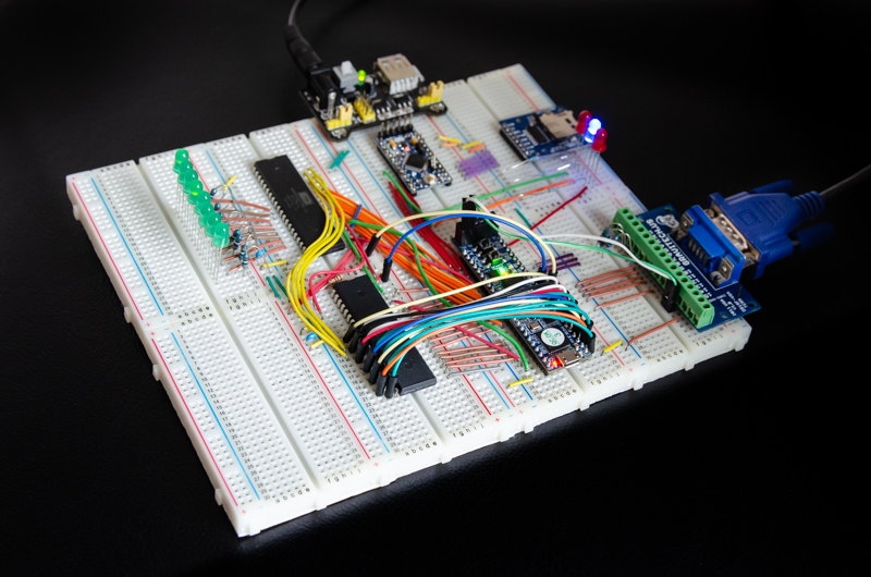
After an 18-month hiatus, I continued work on my homebrew 6502 computer by adding VGA output so that programs can now generate some interesting graphics instead of just turning LEDs on and off.

To accomplish this, the FPGA on the breadboard now contains a new display module that generates a 320×180 picture. At first glance, that’s a bit of an odd resolution. But since I use a widescreen monitor, I opted against 320×200 so that I can fill the whole panel with square pixels. 320×180 is conveniently derived by generating a 1280×720 signal while repeating every pixel and every scan line four times.
My original plan when starting the 6502 project was to leverage the main memory, i.e. the 512 KB SRAM contained on the CMOD A7-15T FPGA module, to hold the framebuffer. The idea was to share the bus in a similar way the C64 handles concurrent memory access. The VIC-II graphics chip in the C64 accesses the bus when the CPU clock is low to fetch image data. The exception is for so-called badlines for which the C64’s 6510 CPU is stopped for a whole scanline while the VIC-II can utilize the bus exclusively.
Instead, I opted for an implementation with separate VRAM that does not appear in the CPU’s address space. The VRAM can be accessed using registers, which in turn are in the CPU’s address space. This is similar to the Vera graphics module used in the 8-Bit Guy’s Commander X16 project. However, my display module is significantly more limited and lacks most of the features that Vera offers.
There are a few advantages to this register-based approach. First and foremost, it is a lot easier to implement since communication between the CPU and the display module works over a handful of memory-mapped I/O ports, similar to the LED output used in the first iteration of this project. That means that there’s no need to get the bus timing right to allow time-multiplexed access to main memory. Next, for larger displays with many colors, it is not necessarily a plus to have the framebuffer in the CPU’s address space. Either the framebuffer takes up a bunch of the address space, or a cumbersome banking scheme needs to be implemented to access pixel data. Similarly, with an 8-bit CPU, addressing a large array of memory is not a particularly convenient endeavor to begin with.
The VRAM is implemented by using the FPGA’s block RAM (BRAM). The BRAM is instantiated as 100KB of dual-port RAM. The first of the two ports is used to write data received over the registers from the CPU into VRAM; this port is clocked using the CPU clock, i.e. Φ₂. Reading back data from VRAM is not implemented yet. The second port is used by the VGA signal generator to read pixel data. Currently, one byte per pixel is read, allowing for a theoretical amount of 256 colors. However, only one bit per color channel is currently wired to the VGA connector (see image below), so that only 8 colors are supported at the moment (red, green, blue, cyan, magenta, yellow, black, and white). The second memory port is clocked with the pixel clock. Both Φ₂ and the pixel clock are synchronized (the latter being a multiple of the former with a slight phase shift) to avoid hold-time violations in the VRAM when access collisions occur between ports.

The display module is controlled over 9 registers, which are mapped starting at $efe0, right before the VIA starting at $eff0. The registers are:
GFX_DATA: data to be written into VRAM (and at some point data to be read)GFX_ALO: low byte of address in VRAM to be written toGFX_AHI: high byte of address in VRAM to be written toGFX_ABK: bank of address (one extra bit is needed to address all 100KB of VRAM)GFX_SLO: low byte start address for top left pixel on screenGFX_SHI: high byteGFX_OLO: low byte of line offsetGFX_OHI: high byteGFX_LRPT: scan line repeat count
Whenever the data register is written to, the value is stored in VRAM to the address determined by ABK, AHI, and ALO. Currently, there’s no auto-increment feature to move to the next byte, so when writing pixels sequentially, these memory addresses need to be incremented accordingly by the CPU. Another consideration to speed things up is to move the registers into the zero page, which will save one cycle when accessing them.
The line offset determines the number of bytes to skip from the first pixel of one line to the first pixel of the next line. In combination with the start address, this allows for scrolling through a playfield that is larger than the viewport both horizontally and vertically.
The line repeat register determines how often each scan line is repeated. For the aforementioned 180 pixels vertical resolution, this register is set to 3 (one line plus three repetitions). Setting it to 0 would yield the full vertical resolution of 720 scanlines for the underlying video mode, but it would also exceed the available VRAM more than twofold. This register is very similar to the CRT Control Maximum Scan Line Register used by the actual VGA standard.
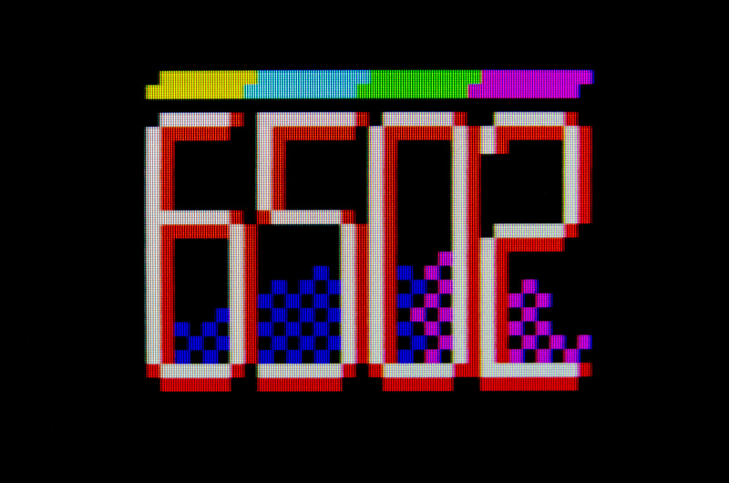
Putting it all together, the CPU can now write pixel data over the graphic module’s registers into VRAM, which then shows up on the monitor. Below is a close-up screenshot of an example using a 32×24 image that I quickly put together in Aseprite. The monitor I’m (ab)using has a native resolution of 1920×1080, so every “breadboard” pixel is displayed as 6×6 physical ones.

In the next blog post, I will show how to squeeze some movement and animation out of the breadboard contraption. Stay tuned — and if you are reading this around the time it was written, stay safe and stay inside.
Subscribe via RSS