VGA from Scratch (Part 1)
It’s time again to leave the realm of Big Data behind for a small electronics project. After generating a VGA signal using an Arduino, I’ve decided to next generate a VGA signal from scratch. From scratch here means using 74HC00 series logic ICs.1
The video mode I picked is XGA at a 60 Hz refresh rate. XGA has a resolution of 1024×768 pixels and a pixel frequency of 65 MHz. By dividing the horizontal resolution by 4, we get a width of 256 pixels and a pixel frequency of 16.25 MHz. To keep the aspect ratio, I am also dividing the vertical resolution by 4, so the effective resolution produced is 256×192.

The generator uses a 16 MHz oscillator, which drives a 9 bit column counter. Counts 0 to 255 are the visible area; then it continues to count up to 335 for the horizontal blanking interval. Based on the count, three signals are generated:
- VISX: active when the generator is not in the horizontal blanking interval,
- HSYNC: the horizontal sync pulse required by VGA,
- EOL: an end-of-line signal to reset the column counter and increase the row counter.
The row counter uses 10 bits to count from 0 to 805 (768 visible rows plus the vertical blanking interval). The two least significant bits are later tossed out to get to the visible vertical resolution of 192 lines. Three signals are derived from the counter:
- VISY: active when the generator is not in the vertical blanking interval,
- VSYNC: the vertical sync pulse required by VGA,
- LASTR: active during the last row in the blanking interval.
When both EOL and LASTR are active, the row counter is reset to start the next frame. When both VISX and VISY are active, then the generator is drawing the visible area and may output pixels. Otherwise, the generator is in a blanking interval and all color channels must be set to black.
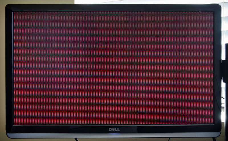
As far as pixel data is concerned, there’s a single NOR gate dedicated to generate an image on screen. It draws red blocks based on one bit each from the column and row counters whenever no blanking occurs. In other words, there isn’t that much going on on the screen just yet.

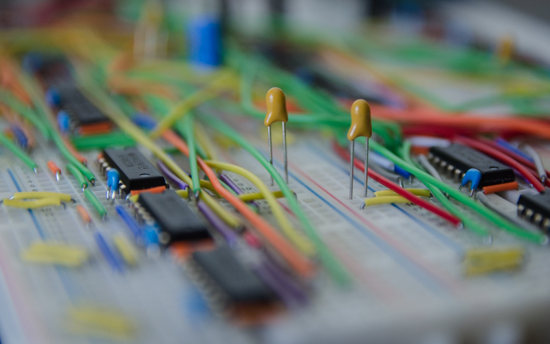
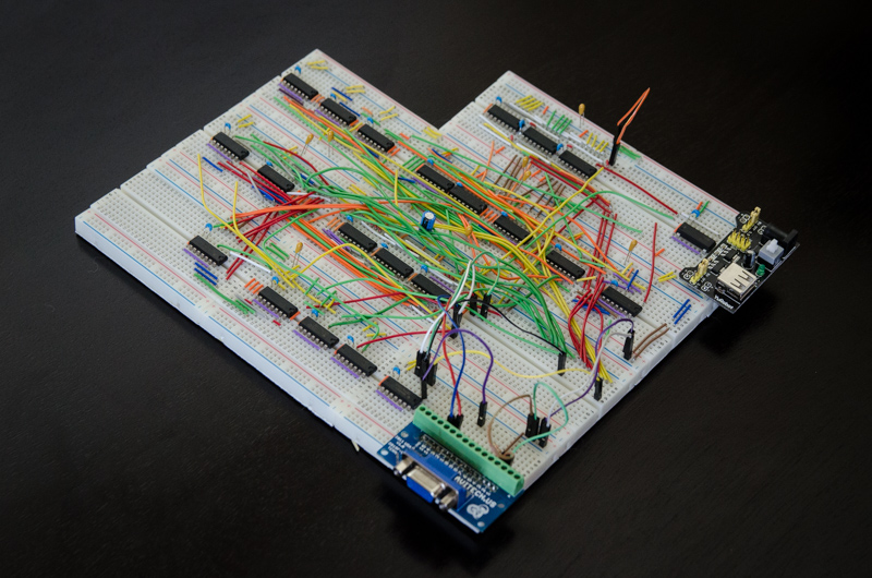
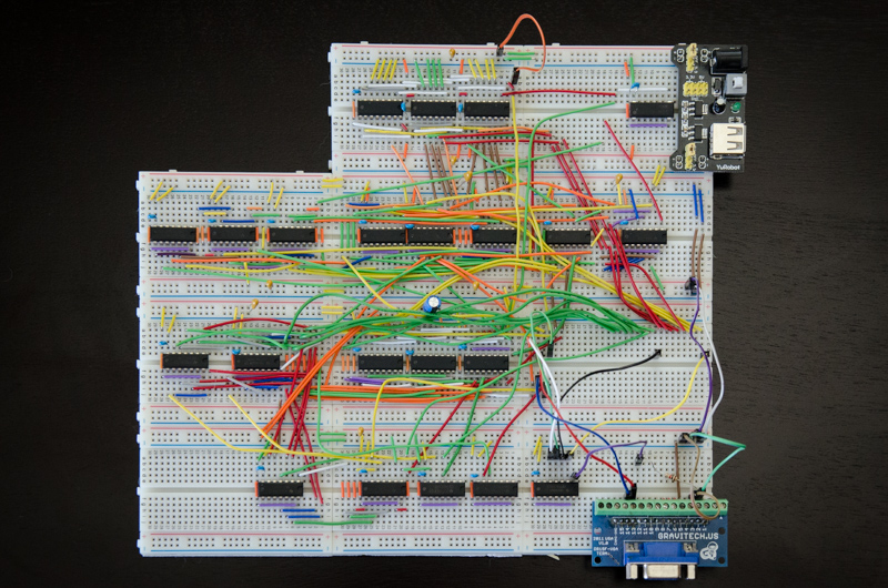
While this looks all fairly straightforward on paper, the implementation on a breadboard actually requires a surprising amount of parts and wires. Here is how it looks right now.


What’s next? Devoting more than a single gate to generate an image would make things more interesting. Also, by adding some dual-port SRAM the generator could become a graphics card for an Arduino, for example. Since both the x and y coordinates fit into a single byte each, addressing the screen will be easy using an 8 bit CPU. As a final observation, I’ve gained a new appreciation of the place-and-route step during FPGA synthesis.
Update: read on in Part 2.
Subscribe via RSS