Homebrew Computer: Adding a 6522 VIA
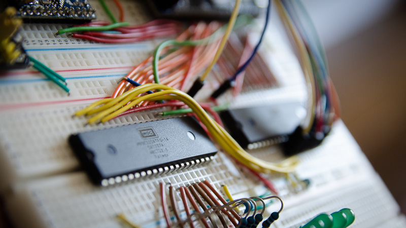
In my last post, I wrote about my first steps towards a 6502-based homebrew 8-bit computer. Since then I’ve added a 6522 Versatile Interface Adapter (VIA). More specifically, it is a W65C22S. The VIA has a number of functionalities (after all, it makes a claim to being versatile).

Most interestingly, it has two 8-bit wide I/O ports (PA and PB) and two timers (T1 and T2). The VIA is operated over 16 registers, which the system’s address decoder currently maps to 0xeff0 to 0xefff.
As a starting point, I hooked up 8 LEDs to PB. While the official data sheet implies that the device can’t drive the LEDs directly, I came across a few online resources that reported more optimistic real-world numbers. For a quick test, connecting the LEDs directly worked, but going forward, I’ll dig up some 74HC-series buffers left over from my VGA generator project.
Using the VIA as LED output has the advantage that the LEDs can be set over the data bus. The only extra GPIO pin of the FPGA that this setup uses is for a chip-select signal (since the address decoder is implemented on the FPGA). That is in contrast to the memory-mapped LEDs I used before, which use up one GPIO pin per LED (for a total of 8 pins).
The VIA also provides two timers that can trigger interrupts on the 6502. The Investigating Interrupts tutorial on 6502.org has been a great resource to get started with the timers. I’ve implemented the moving light shown in my last post using timer interrupts. The VIA implements the timers over 16-bit counters that are decremented at the rate of the CPU clock, and it allows configuring an interrupt signal when a counter reaches zero. Therefore, updating the LEDs on each interrupt would move the light too fast. Instead, the interrupt service routine only updates the light on every tenth interrupt. The following assembly makes it all happen:
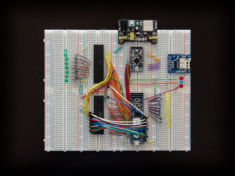
Finally, below is an updated view of the breadboard. The VIA is in the top left with 8 green LEDs connected to PB. The 8 orange wires connect the device to the data bus and the 4 yellow wires connect the 4 lower address bus signals (A0 to A3) to the register select pins of the VIA. The memory mapped LEDs discussed in the last post are the yellow ones in the bottom right, connected to the FPGA board.

Subscribe via RSS