A Modern VIA Connected to a Commodore 64
It has been a while that I embarked on an electronics project (our soldering iron has not seen use since Shannon built her Arduino-powered space pants). For my next project, I decided to hook up a VIA to the expansion port of the Commodore 64 that I put together during the pandemic. What’s a VIA? Well, it’s the Versatile Interface Adapter, an integrated circuit that provides such niceties as timers and GPIO pins to 6502-based systems. I’ve used one in my homebrew 6502 breadboard computer, so this sounded like an easy target. Spoiler alert: there’s still a lot to get wrong, so we won’t see it working in this post just yet. But there’s a lot to learn along the way, so keep on reading if you want to follow along on this journey.
The C64 actually uses two similar chips to interface with various hardware components, the two Complex Interface Adapters (CIAs). These chips are no longer made, but there is an FPGA-based reimplementation available now. In contrast, VIAs are still being manufactured by the Western Design Center (WDC).
The idea of the project is to connect a VIA to the C64 expansion bus and make it appear in the C64’s memory map to leverage its 16 GPIO pins. (The C64 actually already has 9 GPIOs exposed on its user port, which are broken out from one of the CIAs.) To make this work, the address bus needs to be connected to the four register select pins on the chip, the data bus needs to be connected, some address decoding needs to happen (so that the VIA knows when the CPU wants to communicate with it), and then a couple of other signals need to be linked up.
The first challenge is that WDC’s VIA is a CMOS chip and expects CMOS logic levels while the C64’s expansion bus provides TTL-compliant signal levels. For one-directional signals going to the VIA, buffering the signals with a 74HCT244 IC does the trick. The HCT family of devices accepts both CMOS and TTL signal levels as input. The data bus needs to work bidirectionally since the CPU can read and write from the VIA. A 74HCT245 transceiver IC solves that problem, using the read/write signal of the bus to set the direction.
Next, we need address decoding logic to make the VIA’s registers appear in the C64’s memory. The IO1B line of the expansion port goes low if the address on the bus is in the range from 0xde00 to 0xdeff. Wiring this signal to one of the chip select pins of the VIA and to the chip enable pin of the data bus transceiver ensures that the VIA only responds to addresses in this range and that the data bus is disconnected when other components drive it. The four least significant bits of the address bus then get wired to the VIA, and now the VIA’s 16 registers appear starting at 0xde00. (They also repeat 16 times since there are 256 addresses in the IO1B range, but that is not a problem.)
Aside from exposing the two 8-bit ports as headers, I wanted to also include some visual indication and wire the outputs to 16 LEDs. According to its datasheet, the VIA can source 100 mA of current (I am assuming that is across all pins on its ports), so that is getting tight when all 16 LEDs are turned on and when there are additional loads connected to the headers. Instead, I buffer the signals using two more 74HCT244 chips, one for each port. Each can output a total current of 75 mA for a total of 150 mA across both.
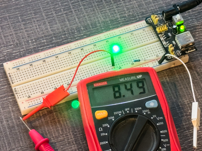
Targeting about 8 mA per LED to stay below the 75 mA if all 8 LEDs on a port are on, that means I need at least a 250 Ω resistor. I ordered a bunch of 261 Ω ones. However, 8 mA is below the suggested input current in the datasheet of the LEDs I bought, which is about 20-30 mA, so I did a quick experiment to see if the brightness is good enough (and what the actual current draw is at 5V). It all checks out (and the LED is quite bright), but the current is slightly higher than anticipated.
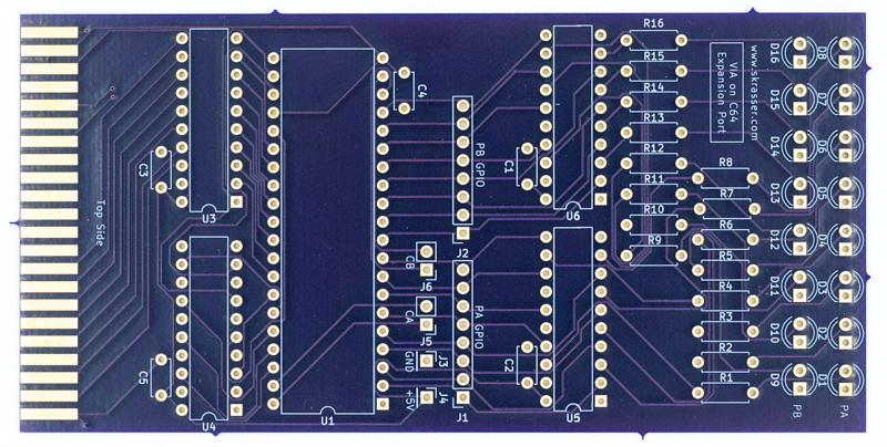
So far so good. The circuit at this point uses one VIA, one 74HCT245 for the data bus, three 74HCT244 chips for buffering various signals, 16 LEDs, and 16 resistors. In addition, each of the 5 ICs needs a decoupling capacitor. Using KiCad, I designed a PCB to connect all of these parts and to provide the edge connector going into the C64 expansion port. I had boards made by OSH Park, a U.S.-based vendor for PCB manufacturing. (For my first PCB adventure a few years back, I went with a Chinese vendor.) For what I needed, this was only slightly more expensive (considering the cheaper postage), but it took a tad longer.
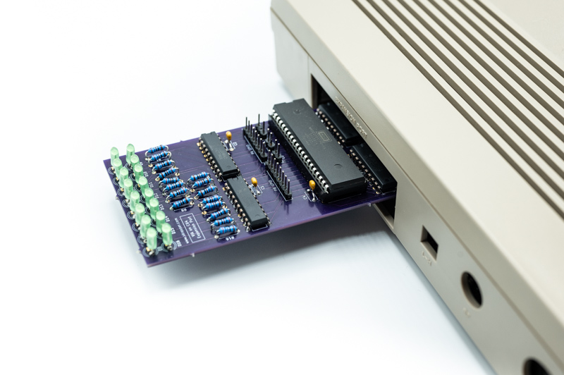
Next, I soldered all the parts to the PCB. For the VIA, I am using a socket. Since that’s the priciest component at about $10, I prefer being able to take it easily off the PCB again. With all the parts added, it was time to give it a spin and plug the board into my C64.
The machine turned on normally, so my next attempt was to access the VIA. To turn on the full second row of LEDs (those connected to Port B of the VIA), the data direction register for that port (DDRB) needs to be set so that all pins act as output. That is Register 2 of the VIA, which should be mapped to 0xde02 or 56834 in decimal. Writing a 255 into that register will do the trick. Next, all pins should be set to high. The output register for the port (ORB) handles that, which is Register 0 mapped to 0xde00 or 56832 in decimal. Again, we need to write a 255. In BASIC, the following commands accomplish this:
  POKE 56834, 255
  POKE 56832, 255
And with that… nothing happened. After closely inspecting the schematic to look for what I could have missed, I noticed that I flipped the address lines coming out of the 74HCT244, reversing their order. That is an annoying yet inconsequential error: it means that Register 2 is now actually mapped to 0xde04 or 56836 in decimal. Still, that did not change anything.
Next, I observed that writing a value to a register did not actually update the register. When writing to DDRB, that value should be able to be retrieved again (it works differently for some other registers). However, writing different values to it did not have any effect. Reading the value (PRINT PEEK(56836)) always returns 255. That is also the behavior for reading/writing to 0xdf00, which is unmapped memory, hence I had a suspicion that the address decoding did not work.
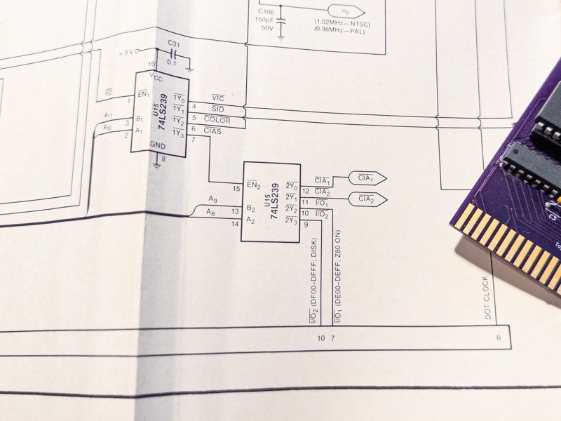
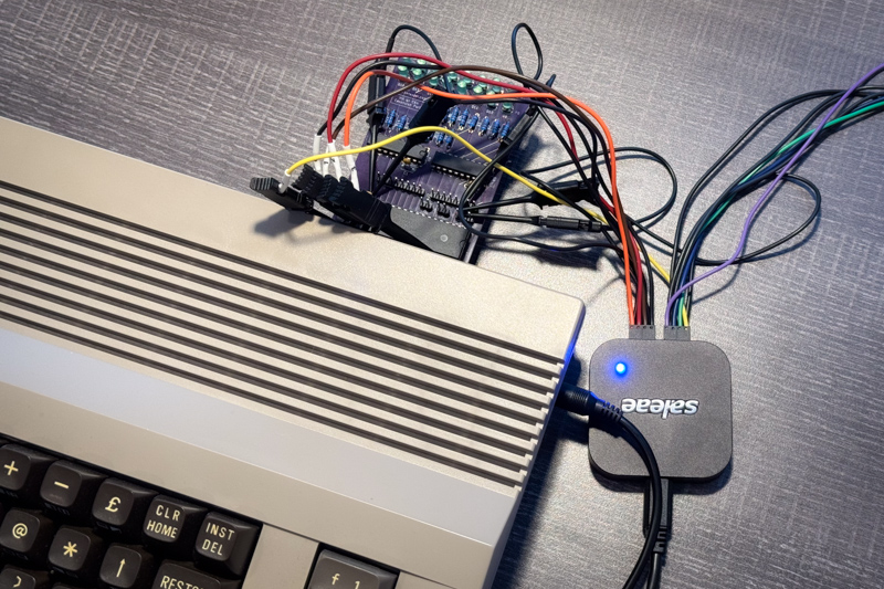
It was time to bust out the logic analyzer. After getting everything set up, I determined that the IO1B line never gets asserted. That did not look right to me, but I wondered if I needed to set any other signals on the expansion port to enable it. However, looking over the C64 schematics in my Programmer’s Reference Guide confirmed that that is not necessary and hence something else is off.
After a while it dawned on me. My C64 uses an Ultimate64 board, an FPGA-based reimplementation of the original hardware with a bunch of convenience features such as virtual cartridges for the expansion port. In the configuration menu of the Ultimate64, I found the “Cartridge Preference” option. Setting it from “Auto” to “External” does the trick. The IO1B line now behaves as expected and drops to low when the address on the bus is in the corresponding range.

With this I was hopeful to get the board working. Alas, I ran into the next issue. Still, none of the LEDs turned on as expected, but I could write to memory and read the written value back—something was now stored on the board since normally no memory is mapped in this area. But interestingly, if I changed the value of one of the VIA registers, I could read that new value back on all of the VIA registers.
Updating all the registers in one write is simply not possible, so something else was going on. Firing up the logic analyzer again, I looked at the address bus signals. From my homebrew 6502 project, I was familiar with the 6502 latching the data bus on the falling edge of its clock, PHI2. I incorrectly assumed that that works similarly for the VIA latching its address and data buses.
Eventually, I looked at the datasheet of the Peripheral Interface Adapter, the W65C21 PIA, a chip similar to the VIA that is also still sold by the Western Design Center. The PIA’s documentation shows a timing diagram for a write cycle. The diagram shows that the address on the address bus needs to be valid shortly before the rising edge and shortly after the falling edge of PHI2, i.e. it needs to be valid for the full duration of PHI2 being high (the same goes for the chip select signals). Assuming that it works similarly for the VIA, I looked again at the data from the logic analyzer. The required signals are valid shortly after the rising edge, so the chip latches the wrong address, although consistently the same wrong one, which results in all reads and writes going to the same register.
The capture below shows that behavior. Since I needed a high temporal resolution (100 MS/s), my device could only support capturing three channels. CS2B is the VIA’s active-low chip select line (the address bus signals look similar though). I have set a trigger on a falling edge on CS2B, i.e. the device starts capturing once the VIA gets selected. Note how this occurs shortly after the rising edge of PHI2.

There are two memory accesses to the VIA in this capture, first a read access right at the trigger point and then a write access immediately after that read (when RWB goes low). This is due to a phantom memory access of the 6502’s STA instruction, which is used to write the accumulator to memory. (The value read is not used.)
So what is different in the C64 that breaks my setup while the VIA worked fine in my homebrew 6502? In the C64’s design, the video chip (VIC) takes control of the bus when PHI2 is low. (There are circumstances where it also assumes control during the half-cycle when PHI2 is high, but we won’t go into that here.) While I was familiar with this aspect, I assumed that the VIC gets out of the way on time when other chips need the bus. After all, there are two CIAs in the machine, and those should work like VIAs or PIAs, should they not?
Well, as it turns out, the CIAs work differently after all. Looking at the CIA datasheet, the address needs to be set at the time when the chip select signal is asserted. The timing diagram shows a setup period (Tads, the time the address bus needs to be set before chip select is asserted), but it is specified as 0 nanoseconds. Hence, the CIAs in the C64 are perfectly fine with the buses not having the right data during the rising edge of PHI2, but the VIA on my board in the expansion port is very much unhappy with this arrangement.
And with that we got to the root of the problem. Now that the issue is understood, we can come up with a solution. Unfortunately, that will mean the PCB will need modifications, yet luckily the $10 VIA will at least come off the board easily. But this will need to wait till the next blog post.
Subscribe via RSS